How to Achieve Ultra-Precision Surface Finish in Lens Molding
Achieving an ultra-precision surface finish in lens molding is critical for high-performance optics in medical, consumer, aerospace, and semiconductor applications. This article reviews the materials, machining technologies, polishing processes, and metrology systems that enable nanometre-level accuracy, and explains how manufacturers can achieve repeatable, ultra-precise results.
1. Why Surface Finish Matters in Lens Molding
In optical manufacturing, surface quality is as important as geometry. To achieve optical-grade lenses, the mold must be finished to nanometre precision, often with roughness values below 10 nm Ra. Without this level of control, light scattering, reduced transmission, and degraded optical performance occur [1].
As global demand grows for compact, high-performance lenses in AR/VR, smartphones, medical imaging, and photolithography, achieving ultra-precision surface finish in lens molding has become a core manufacturing challenge.
2. Key Factors Influencing Ultra-Precision Surface Finish
2.1 Mold Material Selection for Optical Precision
- Nickel–phosphorus (Ni–P) coatings are widely used due to their amorphous microstructure and ability to achieve sub-micron machining accuracy [2].
- Advanced ceramics such as silicon carbide and zirconia offer high thermal stability but require specialist polishing [3].
- Hardened tool steels remain common in injection molding but demand post-processing for nanometre-scale finishes.
2.2 Diamond Turning and Ultra-Precision Machining
Single-point diamond turning (SPDT) is a cornerstone technology in producing mold inserts with nanometre finishes. Equipped with vibration isolation and air-bearing spindles, SPDT machines can achieve:
- Surface roughness <5 nm Ra
- Form accuracies <100 nm
- Repeatability in freeform optics using fast tool servo (FTS) and slow tool servo (STS) [4,5]
This makes SPDT essential for ultra-precision lens molding where freeform and aspheric geometries are required.

2.3 Polishing and Finishing Techniques
Beyond machining, advanced polishing ensures the highest level of optical performance:
- Magnetorheological finishing (MRF): deterministic finishing with nanometre removal rates [6]
- Ion beam figuring (IBF): atomic-scale smoothing with <1 nm roughness [7]
- Plasma-assisted polishing (PAP): ideal for hard optical ceramics [8]
2.4 Process Control During Lens Molding
To maintain optical-grade surface finish during production:
- Temperature control prevents micro-cracks and stress [9]
- Vacuum environments reduce oxidation and contamination [10]
- Protective coatings extend mold life while preserving nanometre precision
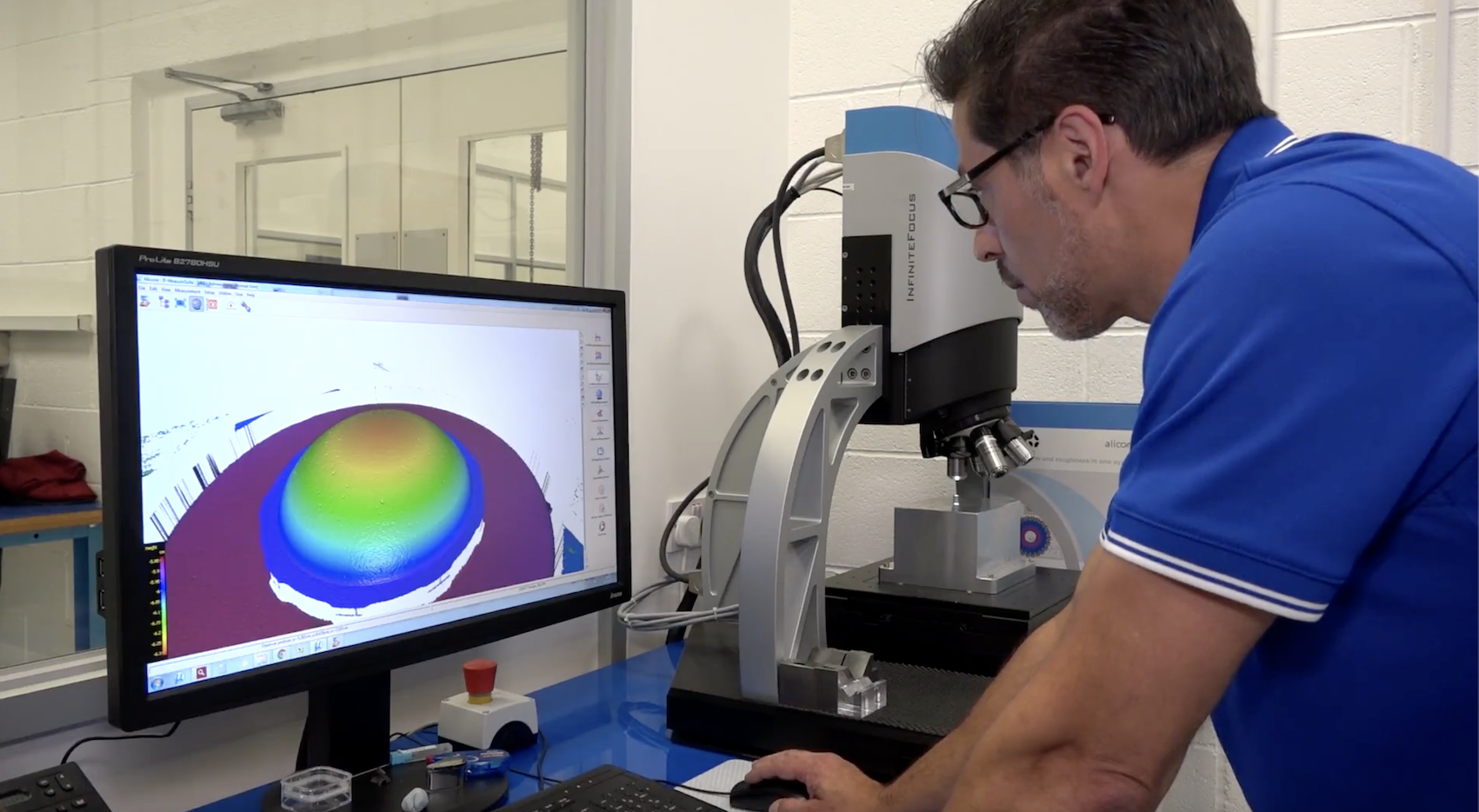
3. Metrology for Verifying Ultra-Precision Finishes
To confirm nanometre-level surface finishes, manufacturers rely on advanced metrology:
- White light interferometry for large-area mapping [11]
- Atomic force microscopy (AFM) for sub-nanometre accuracy [12]
- Power spectral density (PSD) analysis for optical relevance [13]
These tools provide the measurement confidence required for high-volume production of precision optics.
4. Applications of Ultra-Precision Surface Finish in Lens Molding
- Medical optics: endoscopes, intraocular lenses, diagnostic instruments
- Consumer electronics: smartphone lenses, AR/VR freeform optics
- Aerospace and defence: guidance, satellite imaging, surveillance
- Semiconductor lithography: nanometre-precision lenses defining chip patterns
In each case, ultra-precision surface finish directly impacts system efficiency, reliability, and performance.
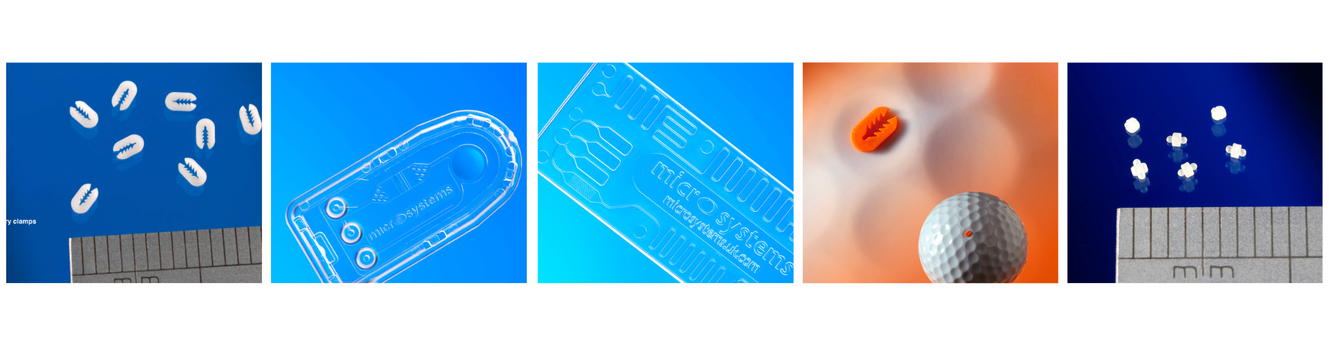
5. How Micro Systems Enables Ultra-Precision Lens Molding
At Micro Systems, we specialise in ultra-precision injection mold tooling for optics and microfluidics. Our expertise includes:
- Diamond machining and polishing delivering <5 nm Ra surface finishes
- Hybrid finishing methods combining SPDT, MRF, and IBF
- Cleanroom manufacturing to eliminate contamination
- In-house metrology with interferometry and AFM for verification
By combining precision engineering, advanced polishing, and rigorous quality assurance, Micro Systems ensures customers achieve repeatable nanometre optical finishes in lens molding, enabling faster product development and superior optical performance.
6. FAQs: Ultra-Precision Surface Finish in Lens Moulding
Q1: What surface roughness is required for optical lens molding?
Typically below 10 nm Ra, with <5 nm Ra required for high-performance optics.
Q2: What technologies are used to achieve ultra-precision finishes?
Diamond turning, magnetorheological finishing (MRF), ion beam figuring (IBF), and plasma-assisted polishing (PAP).
Q3: Why is metrology important in achieving ultra-precision finishes?
Nanometre-scale finishes must be verified with interferometry, AFM, and PSD analysis to ensure optical-grade quality.
Q4: How can Micro Systems support optical manufacturers?
By providing precision mold inserts, advanced finishing, and process support to guarantee ultra-precision replication.
References
[1] M. P. Thompson, Optical Fabrication and Testing, SPIE Press, 2019.
[2] Brinksmeier, E., et al. “Submicron surface finish by precision machining.” CIRP Annals, 1992.
[3] Evans, C. J. and Bryan, J. B., “‘Structured’, ‘Textured’ or ‘Engineered’ Surfaces.” CIRP Annals, 1999.
[4] Shore, P., et al. “Diamond machining of optics: trends and capabilities.” Proc. SPIE 7060, 2008.
[5] To, S., et al. “Precision machining of freeform surfaces with fast tool servo.” Journal of Materials Processing Technology, 2012.
[6] Kordonski, W. I. and Shore, P., “Magnetorheological finishing.” International Journal of Machine Tools and Manufacture, 2006.
[7] Hänsel, T., et al. “Ion beam figuring of optical surfaces.” Applied Optics, 2007.
[8] Mori, Y., et al. “Plasma-assisted polishing of hard optical materials.” Precision Engineering, 2014.
[9] Taga, Y., et al. “Thermal effects on moulded glass optics.” Journal of Non-Crystalline Solids, 2002.
[10] Nishio, K., et al. “Surface coatings for optical moulds.” Thin Solid Films, 2005.
[11] de Groot, P., “Principles of interference microscopy for the measurement of surface topography.” Advances in Optics and Photonics, 2015.
[12] Binnig, G., Quate, C. F., and Gerber, C., “Atomic force microscope.” Physical Review Letters, 1986.
[13] Stover, J. C., Optical Scattering: Measurement and Analysis, SPIE Press, 2012.